How to Create Custom WisBlock Sensor or WisBlock IO Module

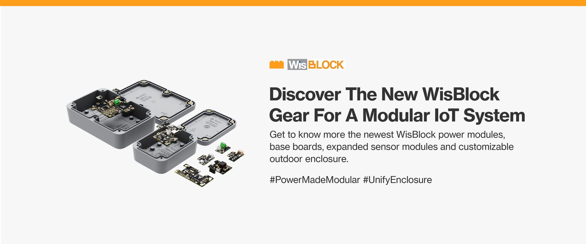
RAKwireless WisBlock is a modular IoT system based on four main blocks.
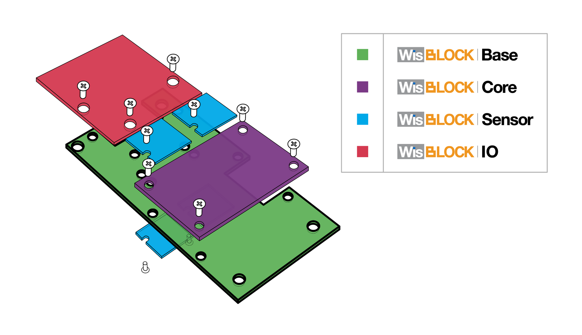
WisBlock Base is the carrier board for the power supply and the inter-connection between the Core, the Sensor and the IO modules.
WisBlock Core is the data processing unit with BLE and LoRa connectivity.
WisBlock IO are interface modules that extend the communication capabilities of WisBlock
WisBlock Sensor are modules that carry different types of sensors with I2C interface.
Custom WisBlock Hardware
WisBlock is growing fast with more and more available IO and Sensor modules. But there might be reasons that you need a variation that is not (yet) available from RAK. Be it that you need a very exotic sensor module or you need an interface technology that is a proprietary product of your company.
We think that IO or Sensor modules that are not available from RAKwireless should not stop you from building your IoT solution based on WisBlock.
WisBlock, as an open source / open hardware project, makes all resources available that are needed to build your own WisBlock custom module.
However, a custom WisBlock module has to be mechanically compatible with the WisBlock system. To make it easier to match the mechanical constraints, we created templates for both WisBlock Sensor and WisBlock IO modules that can be used as the start point. These templates are made with the Autodesk EAGLE™ EDA system, but can be easily transferred to other EDA systems.
The templates include the basic schematic, mechanical outline of the PCB and correct position of the connectors and mounting points. The required board to board connectors are available in libraries for most common EDA systems.
Custom WisBlock Enclosures
Beside of the WisBlock modules, RAKwireless is offering as well a set of enclosures matching the WisBlock mechanical size and fixing points. But for your own product build upon WisBlock modules you might want to choose your enclosure design. To make it easier to design your own enclosure, we provide several examples of indoor and outdoor enclosures as a starting point. And we provide you with the 3D models of the main components of the WisBlock products that you can import in your 3D design application. This makes it easy to check if your custom enclosure has any constraints with the WisBlock modules.
Where to start
Read this first 😄
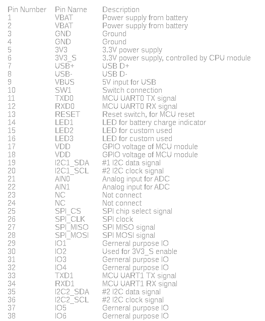
- The board-to-board connectors used in the WisBlock products can be bought from the RAKwireless store. There are two suppliers for the connectors, Panasonic and TXGA. On the base board (RAK19007) are the female/socket version, on the modules are the male/header version
- Panasonic connector data sheet
- TXGA connector female data sheet
- TXGA connector male data sheet
- Download Connector library files
24 pin Connector library files
40 pin Connector library files - Have a good look into the datasheet of the RAK19007 WisBlock Base board to understand the signals connected to the 4 sensor slots. => RAK19007 datasheet
- Have a good look into the datasheet of one of the existing WisBlock Sensor modules to understand the usage of the signals. For example the RAK1906 Environment sensor
- Have a good look into the datasheet of one of the existing WisBlock IO modules to understand the usage of the signals. For example the RAK1920 Sensor Adapter
Make your own WisBlock Sensor board
Template project
To make the task easier, we have prepared a complete example project for Autodesk Eagle™. You can download it as a compressed archive. The project has everything you need to start your own WisBlock Sensor module. It includes the board-to-board connector used on WisBlock Sensor modules and a predefined PCB shape, matching the original WisBlock Sensor modules with the small hole to fix the module to the WisBlock Base board.
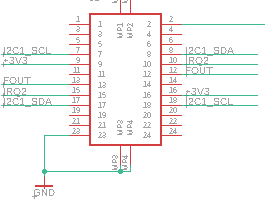
Template schematic
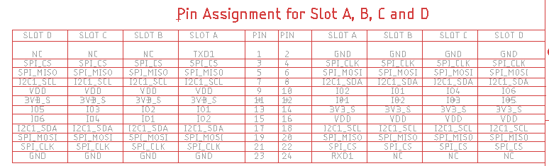
The template schematic is very simple. It only includes the connector and a table that explains the assignment of the pins. As you can see, the connector's pins are assigned in a way that you can rotate the sensor module by 180 degrees if necessary. All 24 pins of the connector are assigned to signals.

Important information about the pin assignments
A few things you need to know.
- VDD is the MCU's GPIO voltage, for a RAK4631 this would be 3.3V. It is available as long as your WisBlock is powered by USB or battery
- 3V3_S is a 3.3V power supply that can be controlled by the WisBlock Core module.
If your sensor module is consuming only a few uA current, you can choose VDD to power the electronic parts of your sensor. But if your module is consuming a higher current, it is strongly recommended to use 3V3_S as supply voltage. This way you can optimize power consumption of your WisBlock application by software. - SPI_MISO, SPI_MOSI, SPI_CLK, SPI_CS signals are for the SPI interface. We recommend not to use SPI on the WisBlock Sensor modules, but instead use I2C. Because the SPI_CS signal is the same on all sensor slots. Only one SPI module can be used on the sensor extension slots of the WisBlock Base board. A workaround could be to use one of the GPIO's available on the sensor slot for the SPI chip select signal.
- RXD1 and TXD1 are only available on slot A of the WisBlock Base board. If your sensor modules requires serial communication, make sure that it is only used in slot A. Also when using the serial signals, the module cannot be plugged in rotated without changes in the software application.
- Depending on the sensor slot the sensor module is plugged in, the connector pins 10, 12, 13 and 15 are connected to different GPIO's (IO1, IO2, IO3, IO4, IO5 and IO6). If you plan to use any of these 4 pins for IRQ or control signals, you have to assign the correct GPIO in your application software.
Check the table for more details:
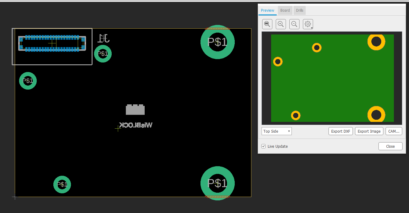
Template PCB
The template PCB matches the size of standard WisBlock Sensor modules. Make sure not to move the connector (bottom side assembly) or the mounting hole that fixes the module on the WisBlock Base board
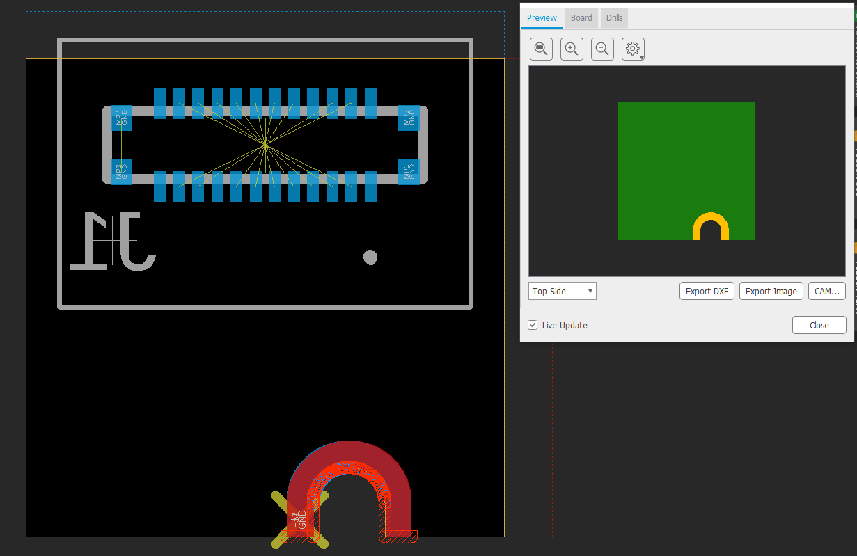
As you can see, Autodesk Eagle™ complains a lot of DRC dimension errors around the mounting whole. The mounting hole and its copper (connected to the GND signal) has to be mechanically located at the edge of the PCB. Autodesk Eagle™ allows only one design rule regarding distance to the PCB edges, hence the DRC errors.
Important information about the PCB design
- As already said, NEVER MOVE THE CONNECTOR AND THE MOUNTING HOLE TO A DIFFERENT LOCATION. If you move them, your self-made WisBlock Sensor will not fit into a WisBlock Base module.
- Due to the small size of the PCB (10 x 10 mm), you might have to change the design rules to use 4 mil connections, 4 mil distance between copper and 0.2 mm via diameters. It will depend on your design if it works with the default Autodesk Eagle™ design rules, but most likely the wires to the connector pads will not be route-able.
- We recommend a GND plane on top and bottom layer.
- Do not place components on the bottom layer. The space between the sensor module and the base board is only 1-2 mm.
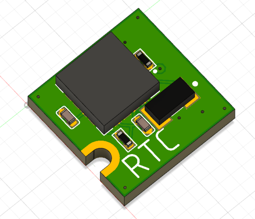
RTC example
For this example I chose a very interesting RTC chip. It is the EnerChip™ CBC34803-M5C RTC module made by CYMBET Corp..
The interesting part is that this chip combines a Real-Time Clock (RTC) and calendar optimized for low power applications with an integrated rechargeable solid state backup battery and all power management functions.
Yes, you read it correct. The chip has an integrated battery. A small one, agreed, it only provides backup of 5 days. But that is already quite good. And there is no need for a large coin battery or a large super capacitor to power the RTC during power down periods.
RTC example schematic
Let's have a look into the WisBlock Sensor RTC schematic.
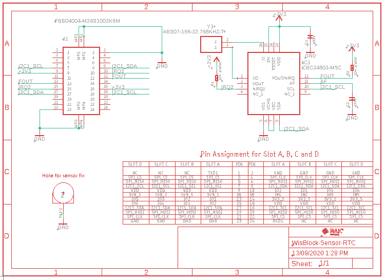
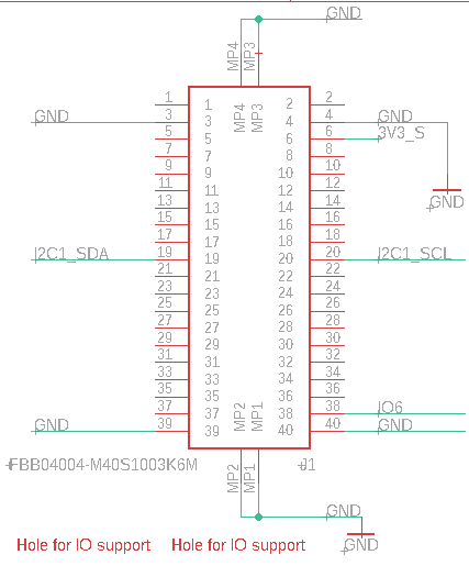
The first thing to check is that we removed most connections from the board-to-board connector.
Only the required nets are left. If you do not remove the unused nets, you will struggle later on in the PCB design because of the mirrored assignment of the signals to the left and right connector row. There will be too many unnecessary connections just between the connector pins.
For the RTC chip, we need only the supply nets, the I2C nets and 2 IRQ lines. The design around the RTC is taken from the datasheet of the EnerChip™ CBC34803-M5C.
RTC example PCB
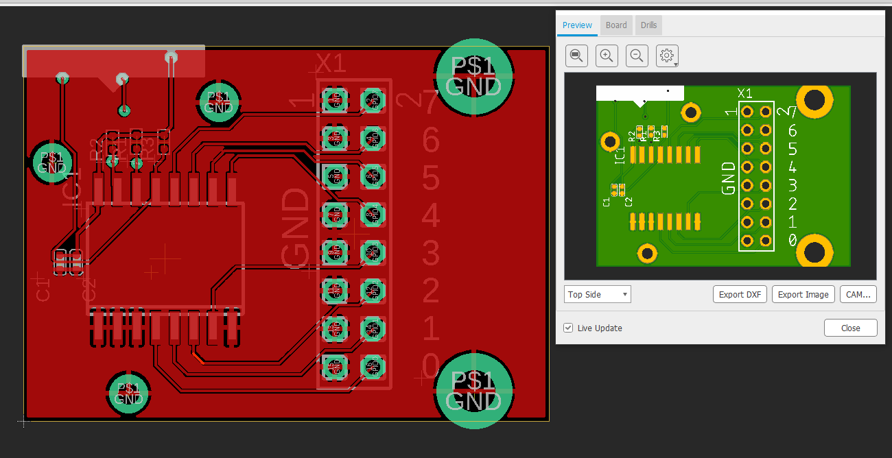
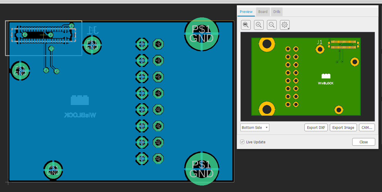
We were able to route the whole design on a two layer board. The connection was so simple, that it could be done with the Autodesk Eagle™ autorouter function. Only one GND connection had to be added manually.
As you can see, we put the recommended GND planes on top and bottom. In addition the open copper area around the mounting hole is visible. This copper area is connected to the GND signal.
RTC top layer

RTC bottom layer

The Eagle files for the RTC example PCB can be downloaded from as a compressed archive
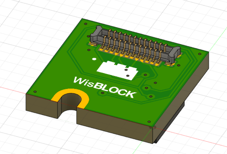
Make your own WisBlock IO board
Template project
To make the task easier, we have prepared a complete example project for Autodesk Eagle™. You can download it as a compressed archive. The project has everything you need to start your own WisBlock IO module. It includes the board-to-board connector used on WisBlock IO modules and a predefined PCB shape, matching the original WisBlock IO modules with the holes to fix the module to the WisBlock Base board.
Template schematic
The template schematic is very simple. It only includes the connector and a table that explains the assignment of the pins. All 38 pins of the connector are assigned to signals. 2 pins are unused
Important information about the pin assignments
A few things you need to know.
- VDD is the MCU's GPIO voltage, for a RAK4631 this would be 3.3V. It is available as long as your WisBlock is powered by USB or battery
- 3V3 is a 3.3V power supply that is available as long as your WisBlock is powered by USB or battery
- 3V3_S is a 3.3V power supply that can be controlled by the WisBlock Core module.
- VBUS is the 5V from the USB connector. This supply is only available while the WisBlock is powered over USB.
- USB+ and USB- are the USB connection from the WisBlock Core module. These signals might not be available on all WisBlock Core modules
- I2C2_SDA and I2C2_SCL are not available on all WisBlock Core modules
- TXD1 and RXD1 are not available on all WisBlock Core modules
If your IO module is consuming only a few uA current, you can choose VDD or 3V3 to power the electronic parts of your IO module. But if your module is consuming a higher current, it is strongly recommended to use 3V3_S as supply voltage. This way you can optimize power consumption of your WisBlock application by software.
Check the table for more details:
Template PCB
The template PCB matches the size of standard WisBlock Sensor modules. Make sure not to move the connector (bottom side assembly) or the mounting holes that fixes the module on the WisBlock Base board
As you can see, Autodesk Eagle™ complains a lot of DRC dimension errors around the larger mounting whole. The mounting hole and its copper (connected to the GND signal) has to be mechanically located at the edge of the PCB. Autodesk Eagle™ allows only one design rule regarding distance to the PCB edges, hence the DRC errors.
If you do not need the whole width (35 mm) for your custom IO module, you can reduce the width and skip the two larger fixing holes on the right side. But make sure that your width covers at least the 3 smaller fixing holes on the left side.
Important information about the PCB design
- As already said, NEVER MOVE THE CONNECTOR AND THE MOUNTING HOLE TO A DIFFERENT LOCATION. If you move them, your self-made WisBlock IO will not fit into a WisBlock Base module.
- Due to the location of the board-to-board connector close to the edge of the PCB, you might have to change the design rules to use 4 mil connections, 4 mil distance between copper and 0.2 mm via diameters. It will depend on your design if it works with the default Autodesk Eagle™ design rules, but most likely the wires to the connector pads will not be route-able.
- We recommend a GND plane on top and bottom layer.
- Do not place components on the bottom layer. The space between the sensor module and the base board is only 1-2 mm.
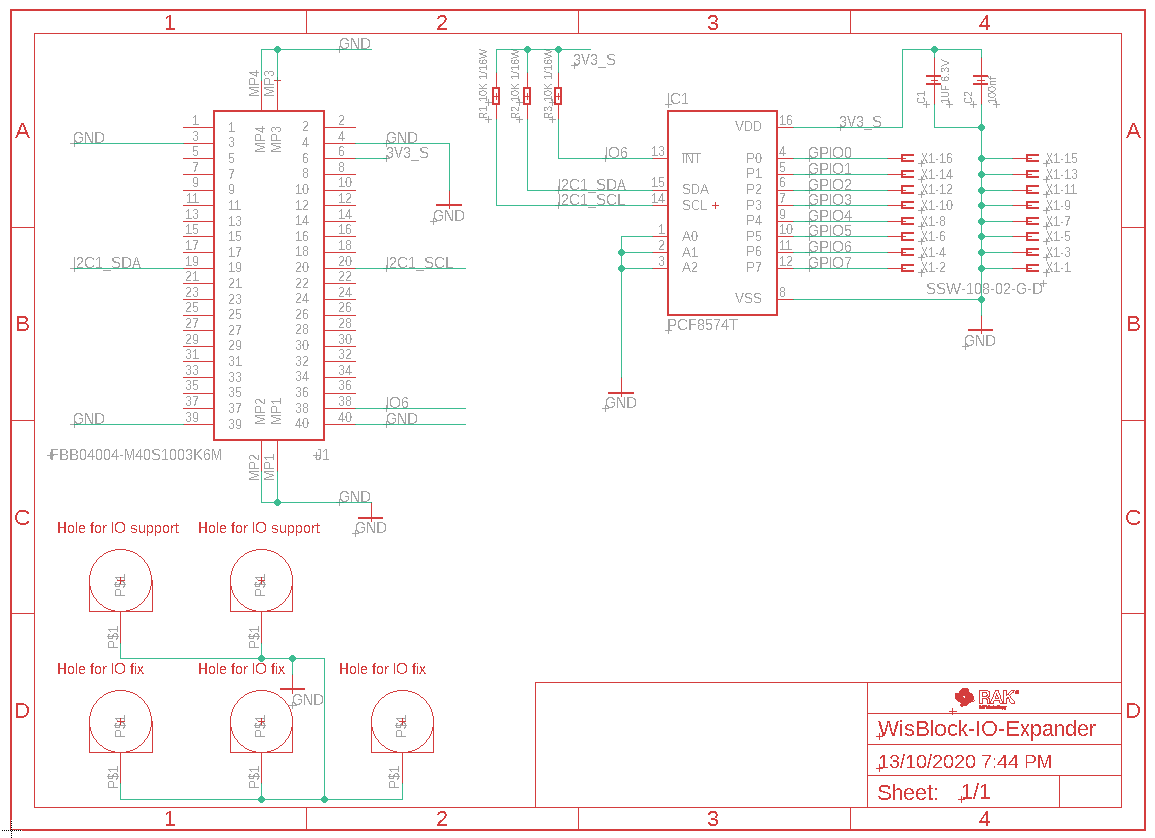
IO Expander example
For this example I chose a very common chip, PCF8574 GPIO expander chip. This chip is controlled over I2C and extends your GPIO count by 8 bi-directional GPIO's.
IO Expander example schematic
Let's have a look into the WisBlock IO expander schematic.

The first thing to check is that we removed most connections from the board-to-board connector.
Only the required nets are left.
For the IO expander chip, we need only the supply nets, the I2C nets and 1 IRQ line. The design around the IO expander is taken from the datasheet of the PCF8574 GPIO expander.
IO Expander example PCB
We were able to route the whole design on a two layer board. The connection was so simple, that it could be done with the Autodesk Eagle™ autorouter function.
As you can see, we put the recommended GND planes on top and bottom. In addition the open copper area around the mounting hole is visible. This copper area is connected to the GND signal.
IO Expander top layer
IO Expander bottom layer
The Eagle files for the IO expander example PCB can be downloaded from as a compressed archive
Make your own WisBlock enclosure
We collected some inspirations for WisBlock compatible enclosures. These examples are tested and should make no problems on your 3D printer.
What you need
All examples have fixing points for the WisBlock Base board and the WisBlock IO modules. For your convenience, we share the 3D STEP files of the RAK5005-O WisBlock Base board and the RAK5801 WisBlock IO module (largest and highest IO module) in the WisBlock 3D folder.
Evaluation Modular
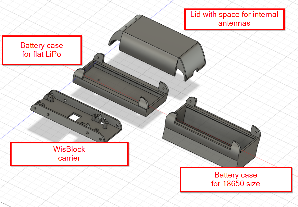
This concept is as modular as the WisBlock itself. It has a WisBlock Base carrier, two versions of battery enclosures and a lid.
The idea is to have a simple enclosure for your WisBlock, which can be used in laboratory or in maker-spaces. This holds your WisBlock Base board and allows easy access to all sensor and IO slots.
Next, is to have a battery enclosure (for 18650 type battery or flat Li-Ion batteries) that can be easily connected to the base carrier.
Finally, a lid that gives basic protection to your WisBlock if you need to take it out for testing.
More details can be found in the Evaluation-Modular folder.
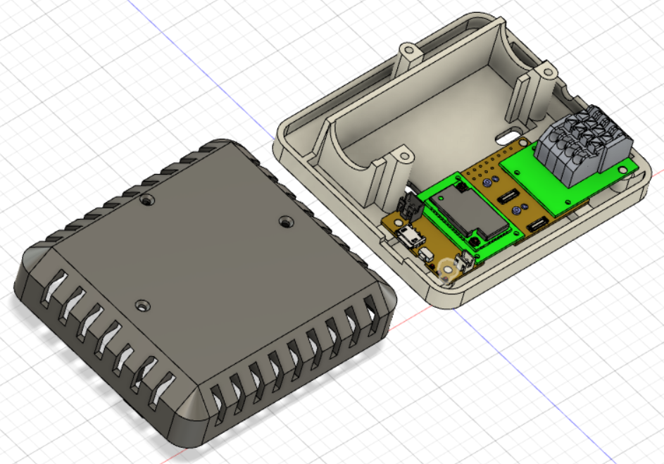
Indoor Environment
This idea was inspired by the RAKBox-B3. As nice as the original enclosure is, it has the problem that it is too small to fit any of the WisBlock IO modules. With this new design, we get a slightly bigger enclosure in width and length, but with a reduced height. Details and 3D files can be found in the Indoor-Environment folder.
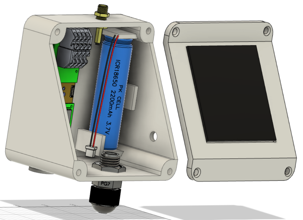
Outdoor Solar
For outdoor usage, it is required to have a certain level of water-proofing. This concept does well in protecting the devices from water damage. However, additional measures must be done to achieve proof standards like IP65.
Most outdoor enclosures, specially the ones with solar panels are not well designed, as the solar panel is often not pointing towards the sky. It causes less efficiency in doing its purpose. This is an approach to make a much more efficient design.
All required files can be found in the Outdoor-Solar folder.
Want to know more about the concept of WisBlock? Download the e-book here.